| Info |
|---|
Depending on the configuration and following revisions, the features of the board are subject to change. For detailed information on hardware specifications, please visit www.seco.com |
This carrier board is contained in the development kit DEV-KIT-SMARC
| Table of Contents | ||
|---|---|---|
|
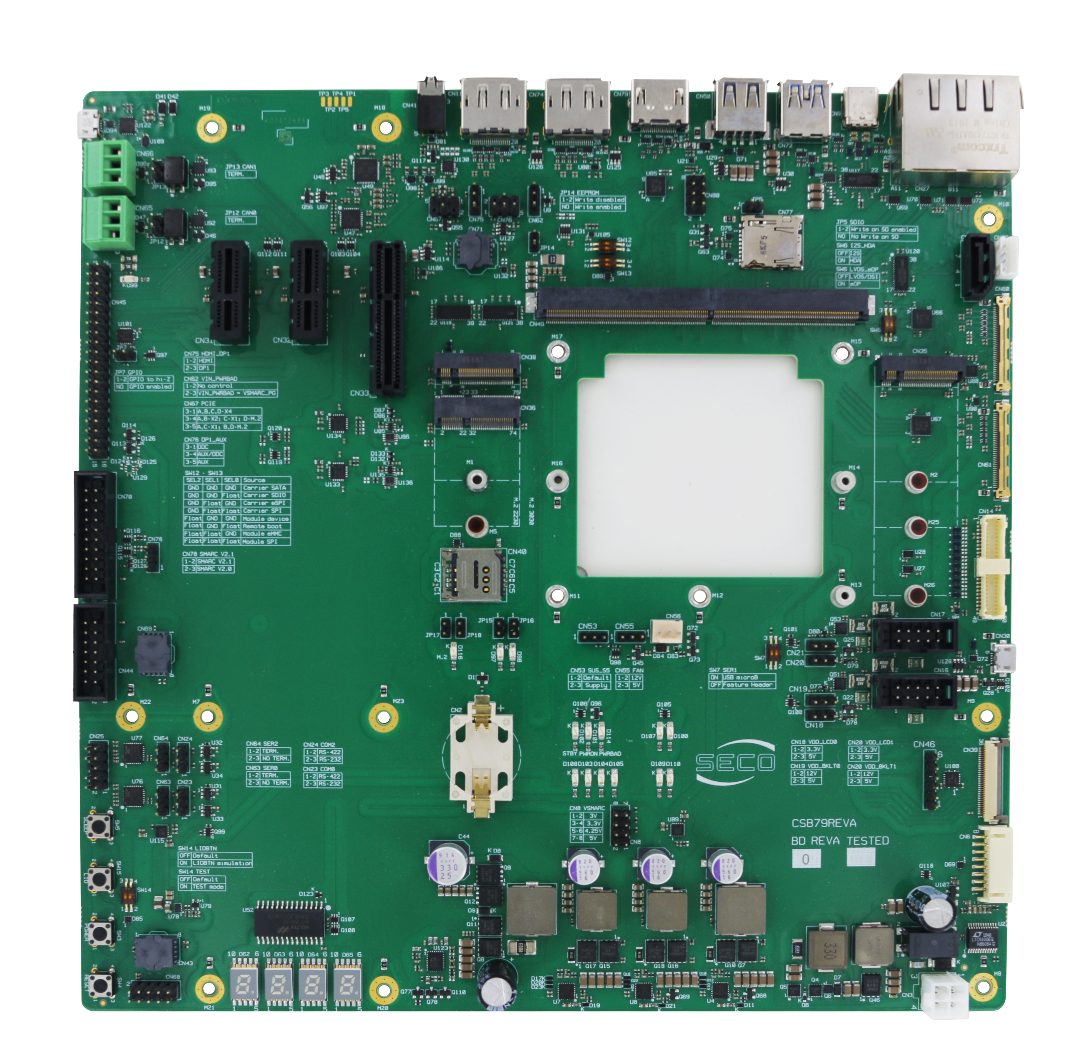
How can I configure jumpers?
Component | Description | Use | Default configuration (Fig.1) |
|---|---|---|---|
CN64 | SER2 | Set no jumper for 120 ohm termination for A-B and Y-Z | Unplugged |
CN63 | SER0 | Set no jumper for 120 ohm termination for A-B and Y-Z | Unplugged |
CN24 | COM2 | Set no jumper for RS-485 | Unplugged |
CN23 | COM0 | Set no jumper for RS-485 | Unplugged |
CN78 | SMARC v2.1 | Set jumper 1-2 for SMARC V2.1 specs | 2-3 Plugged |
JP7 | GPIO | ||
JP12 | CAN0 | Set no jumper no termination | Plugged |
JP13 | CAN1 | Set no jumper no termination | Plugged |
CN67 | PCIE_SEL_AB, PCIE_SEL_CD | Set jumper 3-1 for PCIE A, B, C, D - X4 | 3-5 Plugged |
CN75 | HDMI_DP1#_SEL | Set jumper 1-2 to select HDMI | 1-2 Plugged |
CN76 | DP1_AUX_SEL | Set jumper 3-1 for fixed DDC selection (debug configuration) | 3-1 Plugged |
CN62 | VIN_PWRBAD# | Set jumper 1-2 NO VIN_PWRBAD# control | 1-2 Plugged |
JP14 | I2C EEPROM WP | Set no jumper to enable writes | Unplugged |
JP5 | SDIO_WP | Set no jumper to disable writes on SD Card | 1-2 Plugged |
JP17 | |||
JP18 | |||
JP15 | W_DISABLE1/2#_E | Set no jumper for card enabled | Unplugged |
JP16 | |||
CN53 | SUS_S5 | Set jumper 1-2 for normal operation | 1-2 Plugged |
CN55 | FAN | Set jumper 1-2 for 12V FAN | 1-2 Plugged |
CN8 | VSMARC | Set jumper 1-2 for 3V | 1-2 Plugged |
CN21 | VDD_BKLT1 | Set jumper 1-2 for 12V BKLT Power | 2-3 Plugged |
CN20 | VDD_LCD1 | Set jumper 1-2 for 3.3V Panel Power | 1-2 Plugged |
CN19 | VDD_BKLT0 | Set jumper 1-2 for 12V BKLT Power | 2-3 Plugged |
CN18 | VDD_LCD0 | Set jumper 1-2 for 3.3V Panel Power | 1-2 Plugged |
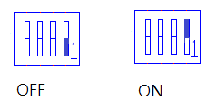
How can I configure micro switches?
Descrpition | Position | Use | Default configuration (Fig.2) |
|---|---|---|---|
SW14 | Position 1-3 | OFF for normal operation ON for test mode | OFF |
Position 2-4 | OFF for normal operation | OFF | |
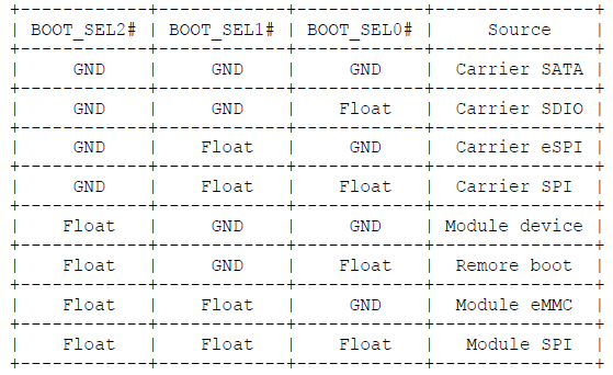
SW12 | Position 1-3 | Fig.3 | OFF |
Position 2-4 | Fig.3 | OFF | |
SW13 | Position 1-3 | Fig.3 | ON |
Position 2-4 | Fig.3 | OFF | |
SW6 | Position 1-3 | OFF for LVDS/DSI | |
Position 2-4 | OFF for I2S | ON | |
SW7 | SER1_SEL | OFF for SER1 - Feature header | OFF |
What to connect and where?
Further information about placement and description of connectors are available here.


